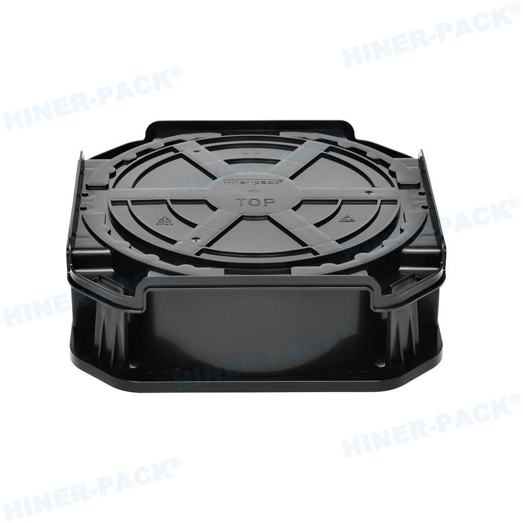
Wafer boxes are specialized containers designed to securely hold, transport, and store semiconductor wafers throughout various stages of the manufacturing process. In the semiconductor industry, where precision, cleanliness, and safety are paramount, wafer boxes play a vital role in preventing contamination, physical damage, and electrostatic discharge (ESD). These high-quality containers are manufactured from cleanroom-compatible materials and engineered to meet the strict handling standards required in modern wafer fabrication and processing facilities. Whether wafers are being transferred between equipment or shipped across the globe, wafer boxes ensure they remain safe, clean, and stable.
The Importance of Wafer Boxes in Semiconductor Manufacturing
Semiconductor wafers are ultra-thin slices of silicon or other materials that serve as the foundation for microchips and integrated circuits. During production, they pass through numerous steps—such as oxidation, etching, lithography, and cleaning—each of which requires careful handling under controlled conditions. Any contamination or mechanical stress can compromise wafer quality, resulting in defects or reduced yield.
Wafer boxes are specifically designed to address these challenges. They provide a secure and sealed environment that shields wafers from particles, dust, moisture, and static electricity. Inside the box, wafers are arranged in precisely molded slots that keep them separated, preventing scratches, chips, or contact with other surfaces. These boxes are essential not only for in-house wafer handling but also for inter-facility and international shipping within the global semiconductor supply chain.
Key Features and Design Specifications
Wafer boxes are built with advanced engineering and high-purity materials to ensure maximum protection and cleanliness. Some of the most important design features include:
- Cleanroom Compatibility: Constructed from low-outgassing polymers like polypropylene (PP) or polycarbonate (PC) that meet ISO Class 5 or better cleanroom standards.
- Anti-Static and ESD Protection: Designed with conductive or static-dissipative materials to prevent electrostatic discharge, which can damage wafer circuits.
- Precision Alignment: Each slot is carefully designed to hold wafers securely in place, maintaining uniform spacing and minimizing movement.
- Sealed Structure: Tight-fitting lids and clasps prevent contamination from airborne particles and moisture.
- Shock and Vibration Resistance: Reinforced exteriors absorb impact and protect wafers during transport.
- Stackable Design: Allows efficient use of space during storage and logistics without compromising safety.
- Custom Sizing: Available in multiple configurations for different wafer diameters (6-inch, 8-inch, 12-inch, etc.) and specific processing needs.
Some wafer boxes are also transparent or translucent, allowing operators to inspect wafers without exposing them to external contaminants.
Applications Across Semiconductor Production and Logistics
Wafer boxes are used across all stages of semiconductor manufacturing and supply chain management. In wafer fabrication plants (fabs), they protect wafers as they are moved between production equipment, ensuring no contamination occurs between process steps. In testing and assembly facilities, wafer boxes keep wafers secure while undergoing electrical inspection, dicing, or packaging.
In global logistics and transportation, wafer boxes are indispensable for shipping wafers between fabrication sites, assembly houses, and clients. They maintain a controlled environment during long-distance transport, ensuring wafers arrive in perfect condition. Additionally, research laboratories use wafer boxes to store and transport prototype or specialty wafers safely.
Benefits of Using Wafer Boxes
Wafer boxes offer numerous advantages that make them essential for the semiconductor industry’s demanding requirements:
- Superior Protection: Prevents physical, electrostatic, and environmental damage.
- Enhanced Cleanliness: Maintains contamination-free conditions required in cleanrooms.
- Improved Efficiency: Simplifies wafer handling, stacking, and transport.
- Durability: Built from strong, chemical-resistant materials that withstand long-term use.
- Cost-Effective: Reduces wafer breakage, contamination, and production losses.
- Sustainability: Reusable design supports eco-friendly manufacturing practices.
- Automation Compatibility: Designed for robotic systems used in modern wafer processing facilities.
By ensuring wafers remain clean and undamaged, wafer boxes directly contribute to higher yields, better product quality, and overall operational efficiency.
Manufacturing and Quality Control Standards
Wafer boxes are produced under strict quality control systems to meet global semiconductor manufacturing standards such as SEMI and ISO. Precision injection molding ensures dimensional accuracy, while each batch undergoes testing for ESD performance, cleanliness, and mechanical durability. Manufacturers also offer customization options, such as color coding, labeling, barcoding, and RFID tracking, to improve traceability and process management.
The best wafer boxes are made in contamination-free environments, ensuring that every unit delivered meets cleanroom certification requirements and supports the stringent demands of wafer fabrication facilities worldwide.
Conclusion
Wafer boxes are an indispensable part of the semiconductor manufacturing ecosystem, providing reliable protection and cleanliness for the most critical component in modern electronics—the silicon wafer. Designed with advanced materials, anti-static protection, and precision alignment, these containers safeguard wafers from the hazards of handling, transportation, and storage. As semiconductor technology advances toward smaller nodes and higher performance chips, the importance of robust and clean wafer protection continues to grow. Durable, efficient, and engineered to perfection, wafer boxes remain a cornerstone of quality assurance and operational excellence in the global semiconductor industry.


